

A | B | C | D | E | F | G | H | CH | I | J | K | L | M | N | O | P | Q | R | S | T | U | V | W | X | Y | Z | 0 | 1 | 2 | 3 | 4 | 5 | 6 | 7 | 8 | 9
| General information | |
|---|---|
| Launched | October 27, 2014 |
| Discontinued | November 2018[1] |
| Marketed by | Intel |
| Designed by | Intel |
| Common manufacturer |
|
| CPUID code | 0306D4h |
| Product code |
|
| Performance | |
| QPI speeds | 6.4 GT/s to 9.6 GT/s |
| DMI speeds | 4 GT/s |
| Cache | |
| L1 cache | 64 KB per core |
| L2 cache | 256 KB per core |
| L3 cache | 2-6 MB (shared) |
| L4 cache | 128 MB of eDRAM (Iris Pro models only) |
| Architecture and classification | |
| Technology node | 14 nm (Tri-Gate) |
| Microarchitecture | Haswell |
| Instruction set | x86-16, IA-32, x86-64 |
| Extensions | |
| Physical specifications | |
| Cores |
|
| GPUs |
|
| Sockets | |
| Products, models, variants | |
| Product code name |
|
| Brand name | |
| History | |
| Predecessors |
|
| Successor | Skylake (Tock/Architecture) |
| Support status | |
| Unsupported | |

Broadwell (previously Rockwell) is the fifth generation of the Intel Core processor. It is Intel's codename for the 14 nanometer die shrink of its Haswell microarchitecture. It is a "tick" in Intel's tick–tock principle as the next step in semiconductor fabrication.[2][3][4] Like some of the previous tick-tock iterations, Broadwell did not completely replace the full range of CPUs from the previous microarchitecture (Haswell), as there were no low-end desktop CPUs based on Broadwell.[5]
Some of the processors based on the Broadwell microarchitecture are marketed as "5th-generation Core" i3, i5 and i7 processors. This moniker is however not used for marketing of the Broadwell-based Celeron, Pentium or Xeon chips. This microarchitecture also introduced the Core M processor branding.
Broadwell is the last Intel platform on which Windows 7 is supported by either Intel or Microsoft; however, third-party hardware vendors have offered limited Windows 7 support on more recent platforms.[6]
Broadwell's H and C variants are used in conjunction with Intel 9 Series chipsets (Z97, H97 and HM97),[7] in addition to retaining backward compatibility with some of the Intel 8 Series chipsets.[citation needed]
Design and variants
Broadwell has been launched in three major variants:[8]
- BGA package:
- Broadwell-Y: system on a chip (SoC); 4.5 W and 3.5 W thermal design power (TDP) classes, for tablets and certain ultrabook-class implementations. GT2 GPU was used, while maximum supported memory is 8 GB of LPDDR3-1600.[9] These were the first chips to roll out, in Q3/Q4 2014. At Computex 2014, Intel announced that these chips would be branded as Core M.[10] TSX instructions are disabled in this series of processors because a bug that cannot be fixed with a microcode update exists.[11]
- Broadwell-U: SoC; two TDP classes – 15 W for 2+2 and 2+3 configurations (two cores with a GT2 or GT3 GPU) as well as 28 W for 2+3 configurations.[12] Designed to be used on motherboards with the PCH-LP chipset for Intel's ultrabook and NUC platforms. Maximum supported is up to 16 GB of DDR3 or LPDDR3 memory, with DDR3-1600 and LPDDR3-1867 as the maximum memory speeds. The 2+2 configuration is scheduled for Q4 2014, while the 2+3 is estimated for Q1 2015.[8] For Broadwell-U models with integrated 5x00 GPUs, die size is 82 mm2 with a total of 1.3 billion transistors, while for the models with 6100 and 6200 GPUs the die size is 133 mm2 with a total of 1.9 billion transistors.
- Broadwell-H: 37 W and 47 W TDP classes, for motherboards with HM86, HM87, QM87 and the new HM97 chipsets for "all-in-one" systems, mini-ITX form-factor motherboards, and other small footprint formats. It was expected to come in two different variants, as single and dual chips; the dual chips (4 cores, 8 threads) would have GT3e and GT2 GPU, while a single chip (SoC; two cores, four threads) would have GT3e GPU. Maximum supported memory is 32 GB of DDR3-1600.[9] These are scheduled for Q2 2015.[8]
- LGA 1150 socket:
- Broadwell-DT: quad-core unlocked desktop version with GT3e integrated graphics (Iris Pro 6200) and 128 MB of eDRAM L4 cache, in a 65 W TDP class. Announced to be backward compatible with the LGA 1150 motherboards designed for Haswell processors.[13]
- LGA 2011-1 socket:
- Broadwell-EX: Brickland platform, for mission-critical servers. Intel QuickPath Interconnect (QPI) is expected to be updated to version 1.1, enabling seamless scaling beyond eight-socket systems. Maximum supported memory speeds are expected to be DDR3-1600 and DDR4-1866.[14][15] Up to 24 core and 48 threads, up to 60 MB of L3 cache and 32 PCI Express 3.0 lanes, with 115–165 W TDP.
- LGA 2011-v3 socket:
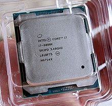
Intel i7 6800K - Broadwell-EP: to be marketed as Xeon E5-2600 v4 etc., while using the C610 Wellsburg chipset platform. Up to 22 cores and 44 threads, up to 55 MB of total cache and 40 PCI Express 3.0 lanes, with 55–160 W TDP classes. Maximum supported memory speed is quad-channel DDR4-2400.[16]
- Broadwell-E: HEDT platform, for enthusiasts. Announced at Computex 2016, it was released in July that year. Consisting of four processors: the 6800K, 6850K, 6900K, and the deca-core 6950X, with clock speeds ranging from 3 GHz to 4 GHz as well as up to 25 MB of L3 cache.

Instruction set extensions
Broadwell introduces some instruction set architecture extensions:[17][18]
- Intel ADX:
ADOXandADCXfor improving performance of arbitrary-precision integer operations[19] RDSEEDfor generating 16-, 32- or 64-bit random numbers from a thermal noise entropy stream, according to NIST SP 800-90B and 800-90C[20]PREFETCHWinstruction[20]- Supervisor Mode Access Prevention (SMAP) – optionally disallows access from kernel-space memory to user-space memory, a feature aimed at making it harder to exploit software bugs.[21]
- Transactional Synchronization Extensions: This instruction set is reintroduced for all versions of Broadwell except for Broadwell-Y because a bug that cannot be fixed via microcode update in Broadwell-Y and all versions of Haswell except for the Haswell-EX variants has been fixed with a new CPU stepping level.[11] Erratum: In fact, among Broadwell i3, i5 and i7 CPUs, only four of them support TSX instructions (i7 5650U and 5600U, i5 5350U and 5300U); it is not even precised on Intel's website whether i5 5200U does support TSX instructions. (ark.intel.com/products/)
New features
Broadwell's Intel Quick Sync Video hardware video decoder adds VP8 hardware decoding[22] and hybrid encoding[23] support.[24] HEVC decode is achieved through a combination of the fixed function video decoder and shaders.[25] Also, it has two independent bit stream decoder (BSD) rings to process video commands on GT3 GPUs; this allows one BSD ring to process decoding and the other BSD ring to process encoding at the same time.[26]
Broadwell's integrated GPU supports on Windows Direct3D 11.2, OpenGL 4.4 (OpenGL 4.5 on Linux[27]) and OpenCL 2.0.[28][29][30] However, it is marketed as Direct3D-12-ready.[31] Broadwell-E introduced Intel Turbo Boost Max Technology 3.0.[32]
List of Broadwell processors
Desktop processors
| Processor branding and model |
Cores (threads) |
GPU model | CPU frequency | TDP | Graphics clock rate | L3 cache | L4 cache[a] | Release date |
Price (USD) |
Socket | |||
|---|---|---|---|---|---|---|---|---|---|---|---|---|---|
| Base | Turbo | Base | Max | ||||||||||
| Core i7 | 5775C | 4 (8) | Iris Pro 6200 | 3.3 GHz | 3.7 GHz | 65 W | 300 MHz | 1.15 GHz | 6 MB | 128 MB | June 2, 2015[33] | $366 | LGA 1150 |
| Core i5 | 5675C | 4 (4) | 3.1 GHz | 3.6 GHz | 1.1 GHz | 4 MB | $276 | ||||||
"Broadwell-E" HEDT (14 nm)
| Model | sSpec number |
Cores | Clock rate | Turbo | L2 cache |
L3 cache |
TDP | Socket | I/O bus | Memory | Release date | Part number(s) |
Release price (USD) |
|---|---|---|---|---|---|---|---|---|---|---|---|---|---|
| Core i7-6950X |
|
10 | 3.0 GHz | 3.5 GHz | 10 × 256 KiB | 25 MB | 140 W
|
LGA 2011-3 | 4 × DDR4-2400 | May 30, 2016 |
|
$1723 | |
| Core i7-6900K |
|
8 | 3.2 GHz | 3.7 GHz | 8 × 256 KiB | 20 MB | 140 W
|
LGA 2011-3 | 4 × DDR4-2400 | Q2 2016 |
|
$1089 | |
| Core i7-6850K |
|
6 | 3.6 GHz | 3.8 GHz | 6 × 256 KiB | 15 MB | 140 W
|
LGA 2011-3 | 4 × DDR4-2400 | Q2 2016 |
|
$617 | |
| Core i7-6800K |
|
6 | 3.4 GHz | 3.6 GHz | 6 × 256 KiB | 15 MB | 140 W
|
LGA 2011-3 | 4 × DDR4-2400 | Q2 2016 |
|
$434 |
Embedded processors
| Processor branding and model |
Cores (threads) |
GPU model | CPU frequency | TDP | Graphics clock rate | L3 cache |
L4 cache[a] |
Release date | Price (USD) |
Socket | |||
|---|---|---|---|---|---|---|---|---|---|---|---|---|---|
| Base | Turbo | Base | Max | ||||||||||
| Core i7 | 5775R | 4 (8) | Iris Pro 6200 | 3.3 GHz | 3.8 GHz | 65 W | 300 MHz | 1.15 GHz | 6 MB | 128 MB | June 2, 2015[33] | $348 | BGA 1364 |
| Core i5 | 5675R | 4 (4) | 3.1 GHz | 3.6 GHz | 1.1 GHz | 4 MB | $265 | ||||||
| 5575R | 2.8 GHz | 3.3 GHz | 1.05 GHz | $244 | |||||||||
| Xeon E3 | 1284Lv4 | 4 (8) | Iris Pro P6300 | 2.9 GHz | 3.8 GHz | 47 W | 1.15 GHz | 6 MB | OEM | ||||
| 1278Lv4 | 2.0 GHz | 3.3 GHz | 800 MHz | 1.0 GHz | $546 | ||||||||
| 1258Lv4 | P5700 | 1.8 GHz | 3.2 GHz | 700 MHz | — | $481 | |||||||
Mobile processors
| Processor branding and model |
Cores (threads) |
GPU model | Base frequency |
Turbo frequency | TDP | cTDP down | Graphics clock rate |
L3 cache |
Release date | Price (USD) | |||
|---|---|---|---|---|---|---|---|---|---|---|---|---|---|
| Single Core | Dual Core | Base | Max | ||||||||||
| Core i7 | 5950HQ | 4 (8) | Iris Pro 6200 | 2.9 GHz | 3.7 GHz | — | 47 W | — | 300 MHz | 1.15 GHz | 6 MB | June 2015 | $623 |
| 5850HQ | Iris Pro 6200 | 2.7 GHz | 3.6 GHz | — | 47 W | — | 300 MHz | 1.1 GHz | 6 MB | June 2015 | $434 | ||
| 5750HQ | Iris Pro 6200 | 2.5 GHz | 3.4 GHz | — | 47 W | 600 MHz / 37 W | 300 MHz | 1.05 GHz | 6 MB | June 2015 | $434 | ||
| 5700HQ | HD 5600 | 2.7 GHz | 3.5 GHz | — | 47 W | 600 MHz / 37 W | 300 MHz | 1.05 GHz | 6 MB | June 2015 | $378 | ||
| 5650U | 2 (4) | HD 6000 | 2.2 GHz | 3.2 GHz | 3.1 GHz | 15 W | 600 MHz / 9.5 W | 300 MHz | 1 GHz | 4 MB | Q1 2015 | $426 | |
| 5600U | HD 5500 | 2.6 GHz | 3.2 GHz | 3.1 GHz | 15 W | Zdroj:https://en.wikipedia.org?pojem=Broadwell_(microarchitecture)||||||||