A | B | C | D | E | F | G | H | CH | I | J | K | L | M | N | O | P | Q | R | S | T | U | V | W | X | Y | Z | 0 | 1 | 2 | 3 | 4 | 5 | 6 | 7 | 8 | 9

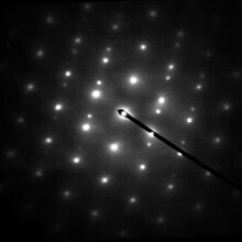
Electron diffraction is a generic term for phenomena associated with changes in the direction of electron beams due to elastic interactions with atoms.[a] It occurs due to elastic scattering, when there is no change in the energy of the electrons.[1]: Chpt 4 [2]: Chpt 5 [3][4] The negatively charged electrons are scattered due to Coulomb forces when they interact with both the positively charged atomic core and the negatively charged electrons around the atoms. The resulting map of the directions of the electrons far from the sample is called a diffraction pattern, see for instance Figure 1. Beyond patterns showing the directions of electrons, electron diffraction also plays a major role in the contrast of images in electron microscopes.
This article provides an overview of electron diffraction and electron diffraction patterns, collective referred to by the generic name electron diffraction. This includes aspects of how in a general way electrons can act as waves, and diffract and interact with matter. It also involves the extensive history behind modern electron diffraction, how the combination of developments in the 19th century in understanding and controlling electrons in vacuum and the early 20th century developments with electron waves were combined with early instruments, giving birth to electron microscopy and diffraction in 1920–1935. While this was the birth, there have been a large number of further developments since then.
There are many types and techniques of electron diffraction. The most common approach is where the electrons transmit through a thin sample, from 1 nm to 100 nm (10 atoms to 1000 thick), where the results depending upon how the atoms are arranged in the material, for instance a single crystal, many crystals or different types of solids. Other cases such as larger repeats, no periodicity or disorder have their own characteristic patterns. There are many different ways of collecting diffraction information, from parallel illumination to a converging beam of electrons or where the beam is rotated or scanned across the sample which produce information that is often easier to interpret. There are also many other types of instruments. For instance, in a scanning electron microscope (SEM), electron backscatter diffraction can be used to determine crystal orientation across the sample. Electron diffraction patterns can also be used to characterize molecules using gas electron diffraction, liquids, surfaces using lower energy electrons, a technique called LEED, and by reflecting electrons off surfaces, a technique called RHEED.
There are also many levels of analysis of electron diffraction, including:
- The simplest approximation using the de Broglie wavelength[5]: Chpt 1-2 for electrons, where only the geometry is considered and often Bragg's law[6]: 96–97 is invoked. This approach only considers the electrons far from the sample, a far-field or Fraunhofer[1]: 21–24 approach.
- The first level of more accuracy where it is approximated that the electrons are only scattered once, which is called kinematical diffraction[1]: Sec 2 [7]: Chpt 4-7 and is also a far-field or Fraunhofer[1]: 21–24 approach.
- More complete and accurate explanations where multiple scattering is included, what is called dynamical diffraction (e.g. refs[1]: Sec 3 [7]: Chpt 8-12 [8]: Chpt 3-10 [9][10]). These involve more general analyses using relativistically corrected Schrödinger equation[11] methods, and track the electrons through the sample, being accurate both near and far from the sample (both Fresnel and Fraunhofer diffraction).
Electron diffraction is similar to x-ray and neutron diffraction. However, unlike x-ray and neutron diffraction where the simplest approximations are quite accurate, with electron diffraction this is not the case.[1]: Sec 3 [2]: Chpt 5 Simple models give the geometry of the intensities in a diffraction pattern, but dynamical diffraction approaches are needed for accurate intensities and the positions of diffraction spots.
A primer on electron diffraction
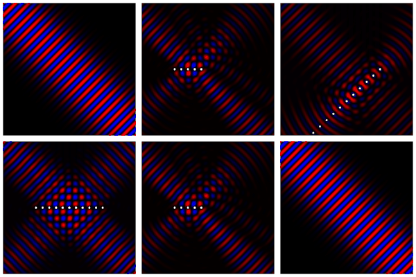
All matter can be thought of as matter waves,[5]: Chpt 1-3 from small particles such as electrons up to macroscopic objects – although it is impossible to measure any of the "wave-like" behavior of macroscopic objects. Waves can move around objects and create interference patterns,[12]: Chpt 7-8 and a classic example is the Young's two-slit experiment shown in Figure 2, where a wave impinges upon two slits in the first of the two images (blue waves). After going through the slits there are directions where the wave is stronger, ones where it is weaker – the wave has been diffracted.[12]: Chpt 1,7,8 If instead of two slits there are a number of small points then similar phenomena can occur as shown in the second image where the wave (red and blue) is coming in from the bottom right corner. This is comparable to diffraction of an electron wave where the small dots would be atoms in a small crystal, see also note.[a] Note the strong dependence on the relative orientation of the crystal and the incoming wave.
Close to an aperture or atoms, often called the "sample", the electron wave would be described in terms of near field or Fresnel diffraction.[12]: Chpt 7-8 This has relevance for imaging within electron microscopes,[1]: Chpt 3 [2]: Chpt 3-4 whereas electron diffraction patterns are measured far from the sample, which is described as far-field or Fraunhofer diffraction.[12]: Chpt 7-8 A map of the directions of the electron waves leaving the sample will show high intensity (white) for favored directions, such as the three prominent ones in the Young's two-slit experiment of Figure 2, while the other directions will be low intensity (dark). Often there will be an array of spots (preferred directions) as in Figure 1 and the other figures shown later.
History
The historical background is divided into several subsections. The first is the general background to electrons in vacuum and the technological developments that led to cathode-ray tubes as well as vacuum tubes that dominated early television and electronics; the second is how these led to the development of electron microscopes; the last is work on the nature of electron beams and the fundamentals of how electrons behave, a key component of quantum mechanics and the explanation of electron diffraction.
Electrons in vacuum
Experiments involving electron beams occurred long before the discovery of the electron; ēlektron (ἤλεκτρον) is the Greek word for amber,[13] which is connected to the recording of electrostatic charging[14] by Thales of Miletus around 585 BCE, and possibly others even earlier.[14]
In 1650, Otto von Guericke invented the vacuum pump[15] allowing for the study of the effects of high voltage electricity passing through rarefied air. In 1838, Michael Faraday applied a high voltage between two metal electrodes at either end of a glass tube that had been partially evacuated of air, and noticed a strange light arc with its beginning at the cathode (negative electrode) and its end at the anode (positive electrode).[16] Building on this, in the 1850s, Heinrich Geissler was able to achieve a pressure of around 10−3 atmospheres, inventing what became known as Geissler tubes. Using these tubes, while studying electrical conductivity in rarefied gases in 1859, Julius Plücker observed that the radiation emitted from the negatively charged cathode caused phosphorescent light to appear on the tube wall near it, and the region of the phosphorescent light could be moved by application of a magnetic field.[17]
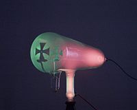
In 1869, Plücker's student Johann Wilhelm Hittorf found that a solid body placed between the cathode and the phosphorescence would cast a shadow on the tube wall, e.g. Figure 3.[18] Hittorf inferred that there are straight rays emitted from the cathode and that the phosphorescence was caused by the rays striking the tube walls. In 1876 Eugen Goldstein showed that the rays were emitted perpendicular to the cathode surface, which differentiated them from the incandescent light. Eugen Goldstein dubbed them cathode rays.[19][20] By the 1870s William Crookes[21] and others were able to evacuate glass tubes below 10−6 atmospheres, and observed that the glow in the tube disappeared when the pressure was reduced but the glass behind the anode began to glow. Crookes was also able to show that the particles in the cathode rays were negatively charged and could be deflected by an electromagnetic field.[21][18]
In 1897, Joseph Thomson measured the mass of these cathode rays,[22] proving they were made of particles. These particles, however, were 1800 times lighter than the lightest particle known at that time – a hydrogen atom. These were originally called corpuscles and later named electrons by George Johnstone Stoney.[23]
The control of electron beams that this work led to resulted in significant technology advances in electronic amplifiers and television displays.[18]
Waves, diffraction and quantum mechanics

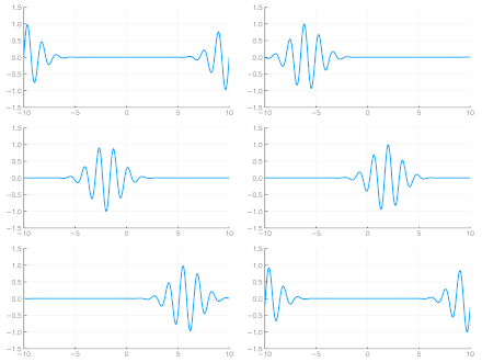
Independent of the developments for electrons in vacuum, at about the same time the components of quantum mechanics were being assembled. In 1924 Louis de Broglie in his PhD thesis Recherches sur la théorie des quanta[5] introduced his theory of electron waves. He suggested that an electron around a nucleus could be thought of as standing waves,[5]: Chpt 3 and that electrons and all matter could be considered as waves. He merged the idea of thinking about them as particles (or corpuscles), and of thinking of them as waves. He proposed that particles are bundles of waves (wave packets) that move with a group velocity[5]: Chpt 1-2 and have an effective mass, see for instance Figure 4. Both of these depend upon the energy, which in turn connects to the wavevector and the relativistic formulation of Albert Einstein a few years before.[24]
This rapidly became part of what was called by Erwin Schrödinger undulatory mechanics,[11] now called the Schrödinger equation or wave mechanics. As stated by Louis de Broglie on September 8, 1927, in the preface to the German translation of his theses (in turn translated into English):[5]: v
M. Einstein from the beginning has supported my thesis, but it was M. E. Schrödinger who developed the propagation equations of a new theory and who in searching for its solutions has established what has become known as “Wave Mechanics”.
The Schrödinger equation combines the kinetic energy of waves and the potential energy due to, for electrons, the Coulomb potential. He was able to explain earlier work such as the quantization of the energy of electrons around atoms in the Bohr model,[25] as well as many other phenomena.[11] Electron waves as hypothesized[5]: Chpt 1-2 by de Broglie were automatically part of the solutions to his equation,[11] see also introduction to quantum mechanics and matter waves.
Both the wave nature and the undulatory mechanics approach were experimentally confirmed for electron beams by experiments from two groups performed independently, the first the Davisson–Germer experiment,[26][27][28][29] the other by George Paget Thomson and Alexander Reid;[30] see note[b] for more discussion. Alexander Reid, who was Thomson's graduate student, performed the first experiments,[31] but he died soon after in a motorcycle accident[32] and is rarely mentioned. These experiments were rapidly followed by the first non-relativistic diffraction model for electrons by Hans Bethe[33] based upon the Schrödinger equation,[11] which is very close to how electron diffraction is now described. Significantly, Clinton Davisson and Lester Germer noticed[28][29] that their results could not be interpreted using a Bragg's law approach as the positions were systematically different; the approach of Hans Bethe[33] which includes the refraction due to the average potential yielded more accurate results. These advances in understanding of electron wave mechanics were important for many developments of electron-based analytical techniques such as Seishi Kikuchi's observations of lines due to combined elastic and inelastic scattering,[34][35] gas electron diffraction developed by Herman Mark and Raymond Weil,[36][37] diffraction in liquids by Louis Maxwell,[38] and the first electron microscopes developed by Max Knoll and Ernst Ruska.[39][40]
Electron microscopes and early electron diffraction
In order to have a practical microscope or diffractometer, just having an electron beam was not enough, it needed to be controlled. Many developments laid the groundwork of electron optics; see the paper by Chester J. Calbick for an overview of the early work.[41] One significant step was the work of Heinrich Hertz in 1883[42] who made a cathode-ray tube with electrostatic and magnetic deflection, demonstrating manipulation of the direction of an electron beam. Others were focusing of electrons by an axial magnetic field by Emil Wiechert in 1899,[43] improved oxide-coated cathodes which produced more electrons by Arthur Wehnelt in 1905[44] and the development of the electromagnetic lens in 1926 by Hans Busch.[45]

Building an electron microscope involves combining these elements, similar to an optical microscope but with magnetic or electrostatic lenses instead of glass ones. To this day the issue of who invented the transmission electron microscope is controversial, as discussed by Thomas Mulvey[46] and more recently by Yaping Tao.[47] Extensive additional information can be found in the articles by Martin Freundlich,[48] Reinhold Rüdenberg[49] and Mulvey.[46]
One effort was university based. In 1928, at the Technical University of Berlin, Adolf Matthias (Professor of High Voltage Technology and Electrical Installations) appointed Max Knoll to lead a team of researchers to advance research on electron beams and cathode-ray oscilloscopes. The team consisted of several PhD students including Ernst Ruska. In 1931, Max Knoll and Ernst Ruska[39][40] successfully generated magnified images of mesh grids placed over an anode aperture. The device, a replicate of which is shown in Figure 5, used two magnetic lenses to achieve higher magnifications, the first electron microscope. (Max Knoll died in 1969,[50] so did not receive a share of the Nobel Prize in Physics in 1986.)
Apparently independent of this effort was work at Siemens-Schuckert by Reinhold Rudenberg. According to patent law (U.S. Patent No. 2058914[51] and 2070318,[52] both filed in 1932), he is the inventor of the electron microscope, but it is not clear when he had a working instrument. He stated in a very brief article in 1932[53] that Siemens had been working on this for some years before the patents were filed in 1932, so his effort was parallel to the university effort. He died in 1961,[54] so similar to Max Knoll, was not eligible for a share of the Nobel Prize.
These instruments could produce magnified images, but were not particularly useful for electron diffraction; indeed, the wave nature of electrons was not exploited during the development. Key for electron diffraction in microscopes was the advance in 1936 where Hans Boersch showed that they could be used as micro-diffraction cameras with an aperture[55]—the birth of selected area electron diffraction.[7]: Chpt 5-6
Less controversial was the development of LEED—the early experiments of Davisson and Germer used this approach.[27][28] As early as 1929 Germer investigated gas adsorption,[56] and in 1932 Harrison E. Farnsworth probed single crystals of copper and silver.[57] However, the vacuum systems available at that time were not good enough to properly control the surfaces, and it took almost forty years before these became available.[58][59] Similarly, it was not until about 1965 that Peter B. Sewell and M. Cohen demonstrated the power of RHEED in a system with a very well controlled vacuum.[60]
Subsequent developments in methods and modelling
Despite early successes such as the determination of the positions of hydrogen atoms in NH4Cl crystals by W. E. Laschkarew and I. D. Usykin in 1933,[61] boric acid by John M. Cowley in 1953[62] and orthoboric acid by William Houlder Zachariasen in 1954,[63] electron diffraction for many years was a qualitative technique used to check samples within electron microscopes. John M Cowley explains in a 1968 paper:[64]
Thus was founded the belief, amounting in some cases almost to an article of faith, and persisting even to the present day, that it is impossible to interpret the intensities of electron diffraction patterns to gain structural information.
This has changed, in transmission, reflection and for low energies. Some of the key developments (some of which are also described later) from the early days to 2023 have been:
- Fast numerical methods based upon the Cowley-Moodie multislice algorithm,[65][66] which only became possible[67] once the fast Fourier transform (FFT) method was developed.[68] With these and other numerical methods Fourier transforms are fast,[69] and it became possible to calculate accurate, dynamical diffraction in seconds to minutes with laptops using widely available multislice programs.
- Developments in the convergent-beam electron diffraction approach. Building on the original work of Walther Kossel and Gottfried Möllenstedt in 1939,[70] it was extended by Peter Goodman and Gunter Lehmpfuhl,[71] then mainly by the groups of John Steeds[72][73][74] and Michiyoshi Tanaka[75][76] who showed how to determine point groups and space groups. It can also be used for higher-level refinements of the electron density;[77]: Chpt 4 for a brief history see CBED history. In many cases this is the best method to determine symmetry.[72][78]
- The development of new approaches to reduce dynamical effects such as precession electron diffraction and three-dimensional diffraction methods. Averaging over different directions has, empirically, been found to significantly reduce dynamical diffraction effects, e.g.,[79] see PED history for further details. Not only is it easier to identify known structures with this approach, it can also be used to solve unknown structures in some cases[80][79][81] – see precession electron diffraction for further information.
- The development of experimental methods exploiting ultra-high vacuum technologies (e.g. the approach described by Daniel J. Alpert in 1953[82]) to better control surfaces, making LEED and RHEED more reliable and reproducible techniques. In the early days the surfaces were not well controlled; with these technologies they can both be cleaned and remain clean for hours to days, a key component of surface science.[82][83]
- Fast and accurate methods to calculate intensities for LEED so it could be used to determine atomic positions, for instance references.[84][85][9] These have been extensively exploited to determine the structure of many surfaces, and the arrangement of foreign atoms on surfaces.[86]
- Methods to simulate the intensities in RHEED, so it can be used semi-quantitatively to understand surfaces during growth and thereby to control the resulting materials.[87]
- The development of advanced detectors for transmission electron microscopy such as charge-coupled device[88] and direct electron detectors,[89] which improve the accuracy and reliability of intensity measurements. These have efficiencies and accuracies that can be a thousand or more times that of the photographic film used in the earliest experiments,[88][89] with the information available in real time rather than requiring photographic processing after the experiment.[88][89]
Core elements of electron diffraction
Plane waves, wavevectors and reciprocal lattice
What is seen in an electron diffraction pattern depends upon the sample and also the energy of the electrons. The electrons need to be considered as waves, which involves describing the electron via a wavefunction, written in crystallographic notation (see notes[c] and[d]) as:[3]
The wavelength of the electrons in vacuum is from the above equations
The magnitude of the interaction of the electrons with a material scales as[1]: Chpt 4
The high-energy electrons interact with the Coulomb potential,[33] which for a crystal can be considered in terms of a Fourier series (see for instance Ashcroft and Mermin),[6]: Chpt 8 that is
Antropológia
Aplikované vedy
Bibliometria
Dejiny vedy
Encyklopédie
Filozofia vedy
Forenzné vedy
Humanitné vedy
Knižničná veda
Kryogenika
Kryptológia
Kulturológia
Literárna veda
Medzidisciplinárne oblasti
Metódy kvantitatívnej analýzy
Metavedy
Metodika
Text je dostupný za podmienok Creative
Commons Attribution/Share-Alike License 3.0 Unported; prípadne za ďalších
podmienok.
Podrobnejšie informácie nájdete na stránke Podmienky
použitia.
www.astronomia.sk | www.biologia.sk | www.botanika.sk | www.dejiny.sk | www.economy.sk | www.elektrotechnika.sk | www.estetika.sk | www.farmakologia.sk | www.filozofia.sk | Fyzika | www.futurologia.sk | www.genetika.sk | www.chemia.sk | www.lingvistika.sk | www.politologia.sk | www.psychologia.sk | www.sexuologia.sk | www.sociologia.sk | www.veda.sk I www.zoologia.sk


