A | B | C | D | E | F | G | H | CH | I | J | K | L | M | N | O | P | Q | R | S | T | U | V | W | X | Y | Z | 0 | 1 | 2 | 3 | 4 | 5 | 6 | 7 | 8 | 9

In electronics, flip-flops and latches are circuits that have two stable states that can store state information – a bistable multivibrator. The circuit can be made to change state by signals applied to one or more control inputs and will output its state (often along with its logical complement too). It is the basic storage element in sequential logic. Flip-flops and latches are fundamental building blocks of digital electronics systems used in computers, communications, and many other types of systems.
Flip-flops and latches are used as data storage elements to store a single bit (binary digit) of data; one of its two states represents a "one" and the other represents a "zero". Such data storage can be used for storage of state, and such a circuit is described as sequential logic in electronics. When used in a finite-state machine, the output and next state depend not only on its current input, but also on its current state (and hence, previous inputs). It can also be used for counting of pulses, and for synchronizing variably-timed input signals to some reference timing signal.
The term flip-flop has historically referred generically to both level-triggered (asynchronous, transparent, or opaque) and edge-triggered (synchronous, or clocked) circuits that store a single bit of data using gates.[1] Modern authors reserve the term flip-flop exclusively for edge-triggered storage elements and latches for level-triggered ones.[2][3] The terms "edge-triggered", and "level-triggered" may be used to avoid ambiguity.[4]
When a level-triggered latch is enabled it becomes transparent, but an edge-triggered flip-flop's output only changes on a clock edge (either positive going or negative going).
Different types of flip-flops and latches are available as integrated circuits, usually with multiple elements per chip. For example, 74HC75 is a quadruple transparent latch in the 7400 series.
History

The first electronic latch was invented in 1918 by the British physicists William Eccles and F. W. Jordan.[5][6] It was initially called the Eccles–Jordan trigger circuit and consisted of two active elements (vacuum tubes).[7] The design was used in the 1943 British Colossus codebreaking computer[8] and such circuits and their transistorized versions were common in computers even after the introduction of integrated circuits, though latches and flip-flops made from logic gates are also common now.[9][10] Early latches were known variously as trigger circuits or multivibrators.
According to P. L. Lindley, an engineer at the US Jet Propulsion Laboratory, the flip-flop types detailed below (SR, D, T, JK) were first discussed in a 1954 UCLA course on computer design by Montgomery Phister, and then appeared in his book Logical Design of Digital Computers.[11][12] Lindley was at the time working at Hughes Aircraft under Eldred Nelson, who had coined the term JK for a flip-flop which changed states when both inputs were on (a logical "one"). The other names were coined by Phister. They differ slightly from some of the definitions given below. Lindley explains that he heard the story of the JK flip-flop from Eldred Nelson, who is responsible for coining the term while working at Hughes Aircraft. Flip-flops in use at Hughes at the time were all of the type that came to be known as J-K. In designing a logical system, Nelson assigned letters to flip-flop inputs as follows: #1: A & B, #2: C & D, #3: E & F, #4: G & H, #5: J & K. Nelson used the notations "j-input" and "k-input" in a patent application filed in 1953.[13]
Implementation

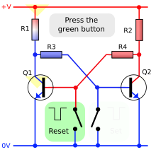
Transparent or asynchronous latches can be built around a single pair of cross-coupled inverting elements: vacuum tubes, bipolar transistors, field-effect transistors, inverters, and inverting logic gates have all been used in practical circuits.
Clocked flip-flops are specially designed for synchronous systems; such devices ignore their inputs except at the transition of a dedicated clock signal (known as clocking, pulsing, or strobing). Clocking causes the flip-flop either to change or to retain its output signal based upon the values of the input signals at the transition. Some flip-flops change output on the rising edge of the clock, others on the falling edge.
Since the elementary amplifying stages are inverting, two stages can be connected in succession (as a cascade) to form the needed non-inverting amplifier. In this configuration, each amplifier may be considered as an active inverting feedback network for the other inverting amplifier. Thus the two stages are connected in a non-inverting loop although the circuit diagram is usually drawn as a symmetric cross-coupled pair (both the drawings are initially introduced in the Eccles–Jordan patent).
Types
Flip-flops and latches can be divided into common types: SR ("set-reset"), D ("data"), T ("toggle"), and JK (see History section above). The behavior of a particular type can be described by the characteristic equation that derives the "next" output (Qnext) in terms of the input signal(s) and/or the current output, .
Asynchronous set-reset latches
When using static gates as building blocks, the most fundamental latch is the asynchronous Set-Reset (SR) latch.
Its two inputs S and R can set the internal state to 1 using the combination S=1 and R=0, and can reset the internal state to 0 using the combination S=0 and R=1.[note 1]
The SR latch can be constructed from a pair of cross-coupled NOR or NAND logic gates. The stored bit is present on the output marked Q.
It is convenient to think of NAND, NOR, AND and OR as controlled operations, where one input is chosen as the control input set and the other bit as the input to be processed depending on the state of the control. Then, all of these gates have one control value that ignores the input (x) and outputs a constant value, while the other control value lets the input pass (maybe complemented):
Essentially, they can all be used as switches that either set a specific value or let an input value pass.
SR NOR latch


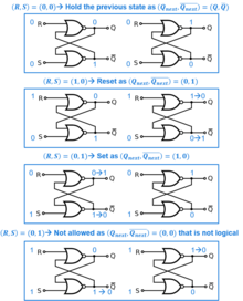
- S = 1, R = 0: Set
- S = 0, R = 0: Hold
- S = 0, R = 1: Reset
- S = 1, R = 1: Not allowed
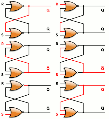
The SR NOR latch consists of two parallel NOR gates where the output of each NOR is also fanned out into one input of the other NOR, as shown in the figure. We call feedback inputs, or simply feedbacks these output-to-input connections. The remaining inputs we will use as control inputs as explained above. Notice that at this point, because everything is symmetric, it does not matter to which inputs the outputs are connected. We now break the symmetry by choosing which of the remaining control inputs will be our set and reset and we can call "set NOR" the NOR gate with the set control and "reset NOR" the NOR with the reset control; in the figures the set NOR is the bottom one and the reset NOR is the top one. The output of the reset NOR will be our stored bit Q, while we will see that the output of the set NOR stores its complement Q.
To derive the behavior of the SR NOR latch, consider S and R as control inputs and remember that, from the equations above, set and reset NOR with control 1 will fix their outputs to 0, while set and reset NOR with control 0 will act as a NOT gate. With this it is now possible to derive the behavior of the SR latch as simple conditions (instead of, for example, assigning values to each line see how they propagate):
- While the R and S are both zero, both R NOR and S NOR simply impose the feedback being the complement of the output, this is satisfied as long as the outputs are the complement of each other. Thus the outputs Q and Q are maintained in a constant state, whether Q=0 or Q=1.
- If S=1 while R=0, then the set NOR will fix Q=0, while the reset NOR will adapt and set Q=1. Once S is set back to zero the values are maintained as explained above.
- Similarly, if R=1 while S=0, then the reset NOR fixes Q=0 while the set NOR with adapt Q=1. Again the state is maintained if R is set back to 0.
- If R=S=1, the NORs will fix both outputs to 0, which is not a valid state storing complementary values.
SR latch operation[4] Characteristic table Excitation table S R Qnext Action Q Qnext S R 0 0 Q Hold state 0 0 0 X 0 1 0 Reset 0 1 1 0 1 0 1 Set 1 0 0 1 1 1 X Not allowed 1 1 X 0
Note: X means don't care, that is, either 0 or 1 is a valid value.
The R = S = 1 combination is called a restricted combination or a forbidden state because, as both NOR gates then output zeros, it breaks the logical equation Q = not Q. The combination is also inappropriate in circuits where both inputs may go low simultaneously (i.e. a transition from restricted to keep). The output could remain in a metastable state and may eventually lock at either 1 or 0 depending on the propagation time relations between the gates (a race condition).

To overcome the restricted combination, one can add gates to the inputs that would convert (S, R) = (1, 1) to one of the non-restricted combinations. That can be:
- Q = 1 (1, 0) – referred to as an S (dominated)-latch
- Q = 0 (0, 1) – referred to as an R (dominated)-latch
This is done in nearly every programmable logic controller.
- Keep state (0, 0) – referred to as an E-latch
Alternatively, the restricted combination can be made to toggle the output. The result is the JK latch.
The characteristic equation for the SR latch is:
- or [14]
where A + B means (A or B), AB means (A and B)
Another expression is:
- with [15]
SR NAND latch

The circuit shown below is a basic NAND latch. The inputs are also generally designated S and R for Set and Reset respectively. Because the NAND inputs must normally be logic 1 to avoid affecting the latching action, the inputs are considered to be inverted in this circuit (or active low).
The circuit uses the same feedback as SR NOR, just replacing NOR gates with NAND gates, to "remember" and retain its logical state even after the controlling input signals have changed. Again, recall that a 1-controlled NAND always outputs 0, while a 0-controlled NAND acts as a NOT gate. When the S and R inputs are both high, feedback maintains the Q outputs to the previous state. When either is zero, they fix their output bits to 0 while to other adapts to the complement. S=R=0 produces the invalid state.
|
 |
SR AND-OR latch

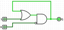
From a teaching point of view, SR latches drawn as a pair of cross-coupled components (transistors, gates, tubes, etc.) are often hard to understand for beginners. A didactically easier explanation is to draw the latch as a single feedback loop instead of the cross-coupling. The following is an SR latch built with an AND gate with one inverted input and an OR gate. Note that the inverter is not needed for the latch functionality, but rather to make both inputs High-active.
SR AND-OR latch operation S R Action 0 0 No change; random initial 1 0 Q = 1 X 1 Q = 0
Note that the SR AND-OR latch has the benefit that S = 1, R = 1 is well defined. In above version of the SR AND-OR latch it gives priority to the R signal over the S signal. If priority of S over R is needed, this can be achieved by connecting output Q to the output of the OR gate instead of the output of the AND gate.
The SR AND-OR latch is easier to understand, because both gates can be explained in isolation, again with the control view of AND and OR from above. When neither S or R is set, then both the OR gate and the AND gate are in "hold mode", i.e., they let the input through, their output is the input from the feedback loop. When input S = 1, then the OR gate outputs 1, regardless of the other input from the feedback loop ("set mode"). When input R = 1 then the AND gate outputs 0, regardless of the other input from the feedback loop ("reset mode"). And since the AND gate takes the output of the OR gate as input, R has priority over S. Latches drawn as cross-coupled gates may look less intuitive, as the behavior of one gate appears to be intertwined with the other gate. The standard NOR or NAND latches could also be re-drawn with the feedback loop, but in their case the feedback loop does not show the same signal value throughout the whole feedback loop. However, the SR AND-OR latch has the drawback that it would need an extra inverter, if an inverted Q output is needed.
Note that the SR AND-OR latch can be transformed into the SR NOR latch using logic transformations: inverting the output of the OR gate and also the 2nd input of the AND gate and connecting the inverted Q output between these two added inverters; with the AND gate with both inputs inverted being equivalent to a NOR gate according to De Morgan's laws.
JK latch
The JK latch is much less frequently used than the JK flip-flop. The JK latch follows the following state table:
JK latch truth table J K Qnext Comment 0 0 Q No change 0 1 0 Reset 1 0 1 Set 1 1 Q Toggle
Hence, the JK latch is an SR latch that is made to toggle its output (oscillate between 0 and 1) when passed the input combination of 11.[16] Unlike the JK flip-flop, the 11 input combination for the JK latch is not very useful because there is no clock that directs toggling.[17]
Gated latches and conditional transparency
Latches are designed to be transparent. That is, input signal changes cause immediate changes in output. Additional logic can be added to a transparent latch to make it non-transparent or opaque when another input (an "enable" input) is not asserted. When several transparent latches follow each other, if they are all transparent at the same time, signals will propagate through them all. However, following a transparent-high latch by a transparent-low latch (or vice-versa) causes the state and output to only change on clock edges, forming what is called a master–slave flip-flop.
Gated SR latch


A gated SR latch can be made by adding a second level of NAND gates to an inverted SR latch. The extra NAND gates further invert the inputs so a SR latch becomes a gated SR latch (a SR latch would transform into a gated SR latch with inverted enable).
Alternatively, a gated SR latch (with non-inverting enable) can be made by adding a second level of AND gates to a SR latch.
With E high (enable true), the signals can pass through the input gates to the encapsulated latch; all signal combinations except for (0, 0) = hold then immediately reproduce on the (Q, Q) output, i.e. the latch is transparent.
With E low (enable false) the latch is closed (opaque) and remains in the state it was left the last time E was high.
A periodic enable input signal may be called a write strobe. When the enable input is a clock signal, the latch is said to be level-sensitive (to the level of the clock signal), as opposed to edge-sensitive like flip-flops below.
|
 |
Gated D latch
This latch exploits the fact that, in the two active input combinations (01 and 10) of a gated SR latch, R is the complement of S. The input NAND stage converts the two D input states (0 and 1) to these two input combinations for the next SR latch by inverting the data input signal. The low state of the enable signal produces the inactive "11" combination. Thus a gated D-latch may be considered as a one-input synchronous SR latch. This configuration prevents application of the restricted input combination. It is also known as transparent latch, data latch, or simply gated latch. It has a data input and an enable signal (sometimes named clock, or control). The word transparent comes from the fact that, when the enable input is on, the signal propagates directly through the circuit, from the input D to the output Q. Gated D-latches are also level-sensitive with respect to the level of the clock or enable signal.
Transparent latches are typically used as I/O ports or in asynchronous systems, or in synchronous two-phase systems (synchronous systems that use a two-phase clock), where two latches operating on different clock phases prevent data transparency as in a master–slave flip-flop.
The truth table below shows that when the enable/clock input is 0, the D input has no effect on the output. When E/C is high, the output equals D.
|
 |
-
Zdroj:https://en.wikipedia.org?pojem=Flip-flop_(electronics)
Text je dostupný za podmienok Creative Commons Attribution/Share-Alike License 3.0 Unported; prípadne za ďalších podmienok. Podrobnejšie informácie nájdete na stránke Podmienky použitia.
Antropológia
Aplikované vedy
Bibliometria
Dejiny vedy
Encyklopédie
Filozofia vedy
Forenzné vedy
Humanitné vedy
Knižničná veda
Kryogenika
Kryptológia
Kulturológia
Literárna veda
Medzidisciplinárne oblasti
Metódy kvantitatívnej analýzy
Metavedy
Metodika
Text je dostupný za podmienok Creative
Commons Attribution/Share-Alike License 3.0 Unported; prípadne za ďalších
podmienok.
Podrobnejšie informácie nájdete na stránke Podmienky
použitia.
www.astronomia.sk | www.biologia.sk | www.botanika.sk | www.dejiny.sk | www.economy.sk | www.elektrotechnika.sk | www.estetika.sk | www.farmakologia.sk | www.filozofia.sk | Fyzika | www.futurologia.sk | www.genetika.sk | www.chemia.sk | www.lingvistika.sk | www.politologia.sk | www.psychologia.sk | www.sexuologia.sk | www.sociologia.sk | www.veda.sk I www.zoologia.sk


